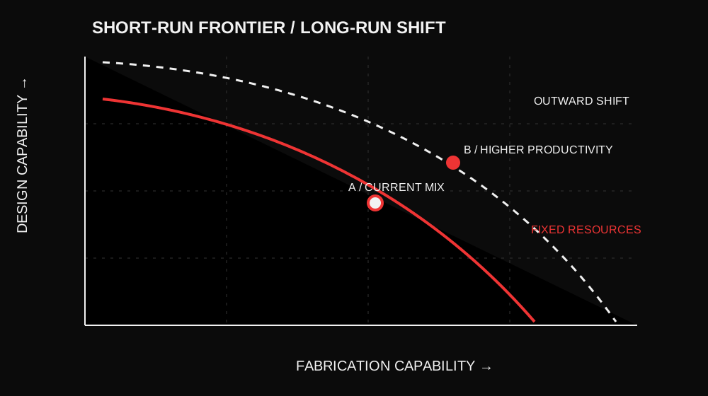
Calling semiconductor strategy a zero-sum game is useful only for a narrow question: with a fixed pool of skilled labor, capital, power, equipment, and time today, what must be deferred to do more of something else? The phrase becomes misleading when used as a permanent description of the industry. Tooling, training, research, trade, and better processes can move the frontier itself. Design and manufacturing also depend on one another; an additional designer is not a substitute for a lithography system.
This article builds a production-possibilities frontier (PPF) as a model, then tests where that model breaks. It does not claim that the plotted units are measured U.S. output. The simulator below uses normalized illustrative values so that the assumptions are visible.
First define the outputs
“Software versus hardware” is too coarse. A useful semiconductor model separates at least four capabilities:
- Design: architecture, RTL, verification, EDA flows, and reusable IP.
- Fabrication: process integration, wafer starts, yield, and equipment utilization.
- Assembly and advanced packaging: substrate, interconnect, thermal design, and test.
- Supporting inputs: chemicals, materials, tooling, utilities, logistics, and trained people.
The outputs do not share a natural unit. A tape-out, a wafer start, and a packaged accelerator are different objects. For an analytical sketch, normalize each to an index of capability. Keep that normalization explicit; otherwise a graph can make incomparable quantities look interchangeable.
NIST describes metrology needs spanning laboratory R&D, prototyping, fabrication, assembly, packaging, and verification. That is a useful warning against treating “making chips” as one stage. NIST’s metrology report also notes that the U.S. led in design and R&D while accounting for roughly 10% of commercial global production at the time of its 2023 assessment. That is a dated observation, not a current market-share estimate.
A deliberately small PPF model
Let a short-run resource budget be $R$. Allocate a fraction $s$ to design and the remainder to fabrication. With diminishing returns, an illustrative model is:
$$D(s)=A(sR)^\alpha,\qquad F(s)=B((1-s)R)^\beta,\qquad 0\le s\le 1$$
Here $D$ and $F$ are normalized capabilities; $A$ and $B$ represent productivity; and $0<\alpha,\beta<1$ creates diminishing marginal returns. Holding $A$, $B$, $R$, and the exponents fixed, varying $s$ traces a frontier. A point inside it suggests unused or poorly matched resources under this model, not proof of real-world inefficiency.
The local slope, $-dF/dD$, is an opportunity-cost measure: how much fabrication capability the model gives up for a small increase in design capability. Because the functions are curved, this cost changes with the starting allocation. Moving engineers between organizations is not instantaneous, however, and capital equipment cannot be reallocated like hours on a calendar. The mathematical slope is a thought experiment, not a staffing instruction.
Explore the frontier
Move the allocation slider. The outputs are normalized model units, not observed national production.
Why the frontier is not the whole supply chain
What the slope actually says
The picture becomes more useful when its slope is derived instead of treated as an abstract “trade-off.” Differentiating the two output equations with respect to $s$ gives
$$\frac{dD}{ds}=A\alpha R^\alpha s^{\alpha-1},\qquad \frac{dF}{ds}=-B\beta R^\beta(1-s)^{\beta-1}.$$
Therefore the marginal rate of transformation, measured as fabrication capability forgone per additional unit of design capability, is
$$-\frac{dF}{dD}=\frac{B\beta}{A\alpha}R^{\beta-\alpha}\frac{(1-s)^{\beta-1}}{s^{\alpha-1}}.$$
This expression forces three questions that a simple curve hides. Are design and fabrication measured in units that make the ratio meaningful? Are the productivity terms stable over the period in question? And can the marginal input actually move between the two activities? If the available resource is a specialized deposition tool, its short-run contribution to design may be effectively zero. A single shared budget $R$ is a simplification, not a literal inventory.
Take the simulator's illustrative settings: $R=100$, $A=B=10$, $\alpha=\beta=0.65$, and $s=0.55$. The model produces roughly 135 design-index units and 119 fabrication-index units. The local trade-off is about 1.07 fabrication-index units per extra design-index unit. That decimal is not a policy recommendation. Change the unit definitions or productivity assumptions and the number moves. Its value is that it tells us exactly which assumptions are doing the work.
The curve is also silent about who bears the opportunity cost. A federal research grant, a private fab expansion, and a university training program do not draw from one perfectly fungible pool. They interact through labor markets, suppliers, power infrastructure, and time. A credible empirical PPF would need to model those constraints separately.
A design becomes a shipped chip only after fabrication, packaging, test, and delivery. If normalized stage capacities are $D$, $F$, $P$, and $T$, a toy bottleneck model is $Q=\min(D,F,P,T)$. The minimum is crude, but it exposes an important point: adding design capacity does little to final throughput when packaging is the limiting stage. The stages are often complements, even when a policy budget must be divided among them.
The bottleneck can shift over time. A higher-yield process increases usable output from the same wafer starts; a packaging advance can unlock a design already waiting for integration; measurement and standards can improve both. NIST specifically identifies advanced packaging, models, interoperability, and supply-chain assurance as metrology priorities. These are not side issues to a design-versus-fab contest; they change the conversion of inputs into usable devices. NIST CHIPS Metrology Program.
Static allocation versus a moving frontier
Three mechanisms can move the frontier outward:
- Productivity: better process control, EDA, simulation, and yield learning raise $A$ or $B$.
- Capacity: new equipment, facilities, power delivery, and trained teams increase the feasible resource base $R$.
- Complementarity: shared standards, packaging, and research reduce coordination losses between stages.
These mechanisms take different amounts of time. A new fab requires long-lived capital and a local ecosystem. A design team may scale differently, but depends on process design kits, EDA tools, and available foundry capacity. Investment can also fail to move the frontier if skilled labor, utilities, or packaging remain scarce. The correct question is therefore not simply “which side wins?” It is “which constraint is binding, over what horizon, and what intervention changes that constraint?”
Yield changes the meaning of capacity
Wafer starts are an input to output, not output itself. If a wafer has $N$ nominal die sites and the fraction passing test is $y$, usable die are approximately $Ny$ before packaging and final test losses. A line running 10% more wafers with poor yield can ship fewer working parts than a line with lower starts and better process control. The details vary by die area, defect density, product mix, binning, and packaging, but the accounting point is general: a “capacity” number needs a conversion chain.
One can extend the toy bottleneck model with yields: $Q\approx\min(D,Fy_f,Py_p,T)$, where $y_f$ and $y_p$ are fabrication and packaging yields. This is still crude. A die that fails one product bin may be sold in another; packages can contain multiple chiplets; different products compete for tools and substrates. The extension is useful because it prevents a common category error: treating an announced wafer-capacity increase as an equal increase in delivered devices.
Learning creates feedback. More production can generate process data; better measurement can improve yield; improved yield can lower cost and support more demand. That means the productivity parameter $B$ may depend on cumulative output, not just today's allocation. A dynamic model might write $B_t=B_0(1+\ell C_t)^\gamma$, where $C_t$ is cumulative learning and $\ell$ is an estimated learning parameter. Without measured data, this is a hypothesis about mechanism, not a number to plug into a headline.
A frontier is conditional on the rest of the world
If imported tools, specialty chemicals, or foreign packaging capacity are required, the feasible domestic output set depends on access to them. A country-level PPF drawn without trade implicitly assumes those links stay available. Conversely, a fully domestic model can hide the efficiency gained through specialization. The question is not whether trade is always good or always bad. It is how a particular dependency changes expected delivery time, recovery time after disruption, and the cost of substitution.
This also matters for intellectual property and design tools. A design organization may appear “asset light,” but its output depends on EDA licenses, foundry design rules, verification infrastructure, and people who know how to use them. An accounting boundary that leaves those inputs outside the picture will make the design frontier look easier to expand than it is.
U.S. business R&D data can inform this question, but expenditure is an input, not a direct measure of technical output. The National Science Foundation’s semiconductor R&D analysis separates industry categories and describes the data source and limitations. It should be read alongside production, yield, trade, workforce, and packaging measures rather than substituted for them.
Comparative advantage has a dependency cost
Specialization can raise aggregate output when organizations focus on what they do well and trade for the rest. In semiconductors, specialization also creates dependencies on foreign or single-source facilities, materials, and expertise. A PPF drawn for one country does not show the resilience of a global supply chain or the cost of a disruption. Nor does a domestic-capacity target automatically imply that every stage should be replicated at any cost.
A more complete decision model would include expected output and exposure to rare interruptions. For example, a planner might compare two feasible portfolios under the same budget:
| Portfolio | Expected short-run output | Disruption exposure | Capability gained |
|---|---|---|---|
| Specialize heavily | Potentially higher | Concentrated supplier risk | Deep expertise in one stage |
| Diversify selectively | Potentially lower initially | Some redundancy | Learning and option value in constrained stages |
Those are directions, not measured outcomes. The actual comparison requires probabilities, recovery times, substitution possibilities, and costs. “Domestic” alone is not a reliability metric; a single domestic site can also fail.
From a line to an investment decision
The short-run PPF is a picture of feasible output given a resource set. Investment changes the set, but investment decisions are made before future demand and technology are known. A planner comparing a packaging facility with an additional design program needs a time-indexed model, not just a point on today's curve. One possible objective is
$$\max_{x_t}\sum_{t=0}^{T}\delta^t\bigl[V(Q_t)-C(x_t)-\lambda L_t\bigr],$$
where $x_t$ is investment, $Q_t$ is delivered output, $C$ is cost, $L_t$ is loss under disruption scenarios, $\delta$ discounts future periods, and $\lambda$ represents how strongly resilience matters. This equation does not solve the policy problem. It states what has to be measured: benefits, costs, timing, and losses under explicit scenarios.
For example, a second supplier may have higher unit cost in normal years yet shorten recovery after a primary supplier outage. The value of that option depends on the chance and duration of disruption, the ability to redesign for another process, inventories, and the cost of waiting. Saying “diversification is safer” without those quantities is as thin as saying “specialization is efficient” without them.
What I would put on the dashboard
If I had to evaluate a real semiconductor policy, I would avoid a single “chip independence” score. I would track separate, dated measures: design starts and tape-out success; installed and utilized wafer capacity by process family; yield-adjusted output; advanced packaging and test throughput; workforce vacancies and training completion; power and water constraints; supplier concentration; and time to qualify an alternate source. Each measure needs a definition and a confidence interval. A national share of global wafer capacity is useful context but cannot stand in for a complete system map.
I would also keep the model falsifiable. If a funded fab reaches its target wafer starts but delivered devices do not rise, the bottleneck model predicts a downstream constraint or a yield problem. If packaging expansion is completed but cycle time does not fall, the assumed constraint may have been wrong. The point of a model is to make a wrong assumption visible soon enough to change course.
How to use the model without overstating it
State the time horizon. A short-run allocation frontier and a decade-long investment frontier are different objects.
Name the constrained resource. Money, skilled labor, cleanroom capacity, water, power, and equipment are not interchangeable.
Measure each stage separately. Design starts, yield-adjusted wafer output, packaging capacity, and delivered devices answer different questions.
Test the bottleneck. If packaging is binding, shifting design resources toward fabrication may not move final deliveries.
Show uncertainty. Use ranges for productivity, demand, and disruption rather than a single precise-looking line.
Separate flows from stocks. Annual R&D spending, installed tools, trained engineers, and shipped devices occupy different parts of the causal chain.
Look for thresholds. Some capabilities are indivisible at small scales; a smooth frontier can be misleading when one new facility or tool changes the feasible set abruptly.
The PPF is valuable because it forces an opportunity-cost question. Its limit is equally valuable: the semiconductor ecosystem is a network of complementary stages whose frontier can move. A useful strategy measures both the trade-off and the mechanisms that make the trade-off less severe.